LAYER STACK & DRILL SPANS
Introduction
The layer stackup defines the physical construction of a PCB: the number of copper layers, the method of fabrication, the materials and thicknesses used, and the dielectric properties of the insulating layers. This information is central to how Proteus manages the board during layout and is used in several ways:
- The layer stackup and board style together determine the legal drill spans. This in turn governs the types of via (through-hole, blind, buried and micro-via) that can be placed during manual and auto-routing.
- The thickness parameters enable Proteus to calculate the physical length of a via for use during length matching operations.
- The complete stackup specification is exported in the CADCAM readme file so that the board manufacturer has a full description of the intended construction.
Users concerned with the EMC performance of their product or working with high-speed signals will typically want to define their PCB layer stack accurately and pass this information through to the fabricator to ensure that board production matches the design intent. The layer stack information is exported in the readme file of all CADCAM output formats and the drill span information is also included in the standard drill plot.
The layer stack should be defined before routing begins. Changing it mid-way through a design requires careful rework of vias and drill spans and is best avoided.
About Layer Stacks
Before looking at how layer stacks are managed in Proteus, it is worth a short recap of terminology and common fabrication options for PCBs.
- Pre-preg is essentially woven fibreglass coated in unset epoxy resin.
- A core is basically ready-made copper-foil/pre-preg/copper-foil or copper-foil/pre-preg.
- A buildup layer is a thin dielectric (typically RCC - Resin Coated Copper) applied to an existing laminate and laser drilled to form micro-vias. This is used only in HDI construction.
A board house will generally have double-sided copper-clad core in stock as a base to start from.
1) They will drill, through-hole-plate and etch one or more of these cores.
2) They will then overlay the board with pre-preg, then either bond that to another core (which could be a basic core or one that has already had additional layers of pre-preg and copper foil applied) or to a copper foil, then they can go back to step 1. Multiple layers of pre-preg can be used together to make up thicker insulating layers.
This process creates a basic set of rules as to what is manufacturable using conventional processes, in particular for drilling. The key principle is that a drill pass can only be performed on material that is accessible to the drilling machine at that stage of the fabrication process. Once layers are bonded together, only the outer surfaces remain accessible.
In Proteus, the board style setting in the Stackup Wizard captures these manufacturing choices. Let's look at each construction method in turn.
Internal Layer Pairs (Inside-Out Construction)
With internal layer construction the board is built outward from a central core. The fabricator starts with a single double-sided core which is drilled, through-hole plated and etched. Pre-preg and copper foil are then laminated to both sides of this core, and the new outer surfaces are drilled and plated. This sequence repeats outward for each additional pair of layers.
With a 4-layer board using internal layer pairs you have one central core. The core is drilled and plated first, then pre-preg and copper foil are applied to each side:
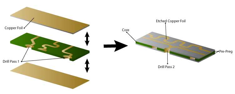
In Proteus, we call this type of stackup internal layer pairs because the cores are built from the inside out.
Because each lamination step buries the previous outer surfaces, the drill opportunities at each stage are limited to the currently exposed faces. For the 4-layer case, the central core (Inner 1 to Inner 2) is drilled before the outer layers exist, and then only a through-board pass is possible after final lamination. Critically, blind vias from the outer copper to the first inner layer (e.g. Top Copper to Inner 1) are not available with internal layer construction because the outer copper foil is laminated directly over pre-preg and there is no fabrication stage at which these two layers form an isolated drillable pair.
With a 6-layer board using internal layer pairs you have two central cores bonded together with pre-preg, then outer pre-preg and foil are applied:
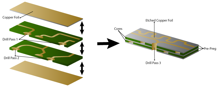
This process extends to 8-layer, 10-layer or 12-layer boards in the same way, with additional cores bonded at the centre and outer layers added last.
External Layer Pairs (Outside-In Construction)
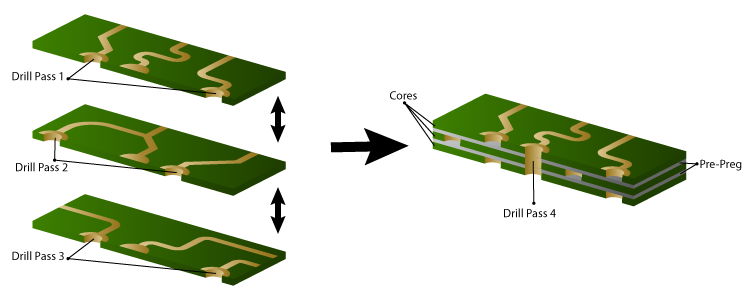
With external layer construction the board is built from multiple pre-fabricated cores that are bonded together. Each core is a double-sided laminate that is individually drilled, through-hole plated and etched before assembly. The completed cores are then stacked with pre-preg between them and laminated in a single press cycle. A final through-board drill and plate pass completes the stackup.
With a 4-layer board using external layer pairs you have two cores, each individually drilled and plated, then bonded together with pre-preg:
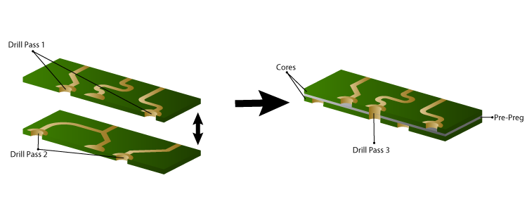
In Proteus, we call this type of stackup external layer pairs because the cores are built from the outside in.
Because each core is drilled independently before lamination, every core provides its own blind or buried drill span. This gives external layer construction the maximum number of blind and buried via options of any conventional method.
With a 6-layer board using external layer pairs you have three cores, each individually drilled and plated, then all bonded together with pre-preg:
1+n+1 HDI (Single Buildup)
The 1+n+1 designation describes a board with one laser-drilled buildup layer on each side of a conventional multi-layer core. The 'n' in the name refers to the number of inner copper layers in the central core section, not the total layer count. A 1+n+1 board with n=2 (two inner layers) has four copper layers in total: Top Copper, Inner 1, Inner 2 and Bottom Copper, where Top-to-Inner1 and Inner2-to-Bottom are laser-drilled micro-via spans and Inner1-to-Inner2 is the mechanically drilled core.
The fabrication process begins with the central core section which is manufactured using conventional techniques (mechanical drilling and plating, using internal or external layer construction as appropriate for the core layer count). Thin buildup dielectric layers (typically RCC) are then laminated to both sides of the completed core. A laser drills the micro-via holes through the buildup dielectric, and these are then plated to form electrical connections between the outer copper and the first inner layer.
Note that it is also possible to create different stackups using fewer cores and more pre-preg with laser drilling passes. This is more complex, more expensive to make and less common but is discussed in the topic on custom layer stacks.
Manufacturing and Cost Considerations
The choice of board style has a direct and significant impact on what can be manufactured, the cost of fabrication and the engineering performance of the finished board. Understanding these factors before selecting a board style will avoid costly redesign later in the project.
Drill Constraints by Board Style
Each construction method imposes constraints on the drill spans, via types and minimum hole sizes that are achievable. The fundamental rule is that a drill pass can only be performed on material that is accessible to the drilling machine at that point in the fabrication sequence.
Internal Layers
Because the outer copper is the last layer applied, there is no fabrication stage at which a blind via from the surface to the first inner layer can be drilled. The available drill spans are limited to buried vias within individual cores (drilled before lamination) and through-hole vias (drilled after final lamination). For a 4-layer internal construction the legal spans are:
- Top Copper to Bottom Copper (through-hole) - drilled after final lamination.
- Inner 1 to Inner 2 (buried via) - drilled through the central core before the outer layers are applied.
For a 6-layer internal construction the additional spans are: Inner 1 to Inner 2 (buried, first core), Inner 3 to Inner 4 (buried, second core), and Inner 1 to Inner 4 (drilled after the two cores are bonded but before the outer foil is applied).
Mechanically drilled vias on internal layer boards typically use drill sizes of 0.2 mm (8 mil) and above. Drill sizes are constrained by the depth being drilled through and the aspect ratio limits of the fabricator (typically 8:1 to 10:1 for standard processes).
Internal layer construction is well suited to designs that need buried vias between inner layer pairs but do not require blind vias from the surface. It tends to produce a more symmetrical stackup which is beneficial for controlling bow and twist.
External Layers
Because each core is drilled independently before lamination, every core provides its own blind or buried drill span. For a 4-layer external construction the legal spans are:
- Top Copper to Bottom Copper (through-hole) - drilled after final lamination.
- Top Copper to Inner 1 (blind via) - drilled through the top core before lamination.
- Inner 2 to Bottom Copper (blind via) - drilled through the bottom core before lamination.
For a 6-layer external construction the additional spans are: Top Copper to Inner 1 (blind), Inner 2 to Inner 3 (buried), and Inner 4 to Bottom Copper (blind).
All drill passes use mechanical CNC drilling. Minimum hole sizes are typically 0.2 mm (8 mil) for through-hole and blind vias, with some fabricators capable of 0.15 mm (6 mil) for blind spans where the aspect ratio is favourable. Blind vias can only span a single core thickness.
External layer construction is the most common choice for multi-layer boards that need blind and buried vias without the cost of HDI laser drilling. It provides the greatest flexibility in drill span options using conventional mechanical processes.
1+n+1 HDI
The outer-to-first-inner spans (e.g. Top Copper to Inner 1) are laser drilled micro-via spans. The inner core section has its own mechanical drill spans for the cores within it. For a 1+2+1 board (four total copper layers) the legal spans are:
- Top Copper to Bottom Copper (through-hole) - mechanically drilled after all lamination is complete.
- Top Copper to Inner 1 (micro-via) - laser drilled through the top buildup layer.
- Inner 1 to Inner 2 (buried via) - mechanically drilled through the central core.
- Inner 2 to Bottom Copper (micro-via) - laser drilled through the bottom buildup layer.
Micro-vias are significantly smaller than mechanically drilled holes. Typical micro-via diameters are 0.075 mm to 0.15 mm (3 to 6 mil) with the most common size being 0.1 mm (4 mil). The buildup dielectric must be thin enough for the laser to drill cleanly, typically 0.04 mm to 0.1 mm (1.5 to 4 mil). The aspect ratio of a laser-drilled micro-via, that is its depth divided by its hole diameter, is what limits it to a single buildup layer in a 1+n+1 construction. Proteus applies the IPC-2226 figures when it checks the board: a micro-via whose aspect ratio exceeds 0.75:1 raises a warning, and one that exceeds 2:1 is reported as a failure. Aim for 0.75:1 or below and discuss anything above that with your fabricator before committing to it.
Proteus also applies hole size constraints automatically when a via is edited to use a micro-via style. The hole is held between 3 thou (0.075 mm) and 8 thou (0.2 mm), and the via is forced to filled, since micro-vias are copper filled as part of the HDI fabrication process. See Editing Vias below.
It is not possible to place a mechanically drilled via on a micro-via span (e.g. Top Copper to Inner 1) because the buildup layer is too thin for reliable mechanical drilling. If your design requires a larger via on this span, you must use a through-hole via that spans the entire board. This is an important design constraint: on a 1+n+1 board the only via options between the outer copper and first inner layer are micro-vias or full through-hole vias.
Engineering Trade-Offs
- Cost and lead time: Each additional lamination cycle or drill pass adds cost and complexity. Blind and buried vias require sequential lamination and are significantly more expensive than through-hole only construction. HDI fabrication requires laser drilling equipment and additional process steps which typically adds 30-50% to the board cost compared with conventional construction of the same layer count.
- Standard stackups: Board houses often provide a list of standard stackups. Using these can reduce cost and lead times compared with custom constructions.
- Impedance control: For impedance-controlled designs, tolerances on dielectric thickness and material constant (εr) should be agreed with your fabricator. Typical variations are ±10%.
- Mechanical rigidity: Adding more copper layers increases rigidity but can also create risks of bow and twist if copper distribution is unbalanced. HDI buildup layers add minimal structural rigidity compared to conventional cores; the central core section provides the primary stiffness.
- Thermal performance: Micro-vias have a much smaller cross-sectional area of copper than mechanical vias, which limits their ability to conduct heat between layers. For thermal management applications, mechanical through-hole vias or dedicated thermal vias are more effective.
- Signal integrity: Micro-vias have significantly lower parasitic inductance and capacitance than through-hole vias because of their shorter length and smaller geometry. This makes them advantageous for high-speed digital signals where via stub effects would otherwise degrade signal quality.
- Power delivery: Through-hole vias remain the preferred method for power and ground connections that must carry significant current. Micro-vias can be used in arrays but this consumes routing space on the buildup layers.
- Symmetry: A symmetrical stackup is important in all constructions to prevent warping during thermal cycling. The buildup layers on an HDI board should be of equal thickness on both sides and copper distribution should be balanced across the board cross-section.
1+n+1 HDI is most commonly chosen when fine-pitch BGA escape routing demands it. If your design can be routed with conventional blind and buried vias using external layer construction, this will generally be less expensive and faster to manufacture.
Key Points
- You need to decide how the board is to be constructed (internal layer pairs, external layer pairs or 1+n+1 HDI). Proteus can then define the stack for you in the Stackup Wizard.
- The construction of the layer stack is crucial in determining valid drill passes. In turn, this determines what types of via you can use in the PCB. Proteus can set this up for you via the drill span dialogue.
- If at all possible, you want to set up the layer stack before you start placing and routing the PCB. Changing the layer stack mid-way through design is fraught with danger and needs careful thought.
Defining a Layer Stack
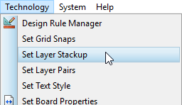
In Proteus, layer stack setup forms part of the New Project Wizard to ensure that the stackup is defined before PCB layout begins. Alternatively, you can set it up at any time from the Set Layer Stackup command on the Technology Menu.
If you define the layer stack in one of your PCB templates then each time you start a project from that template the stackup will already be defined.
The dialogue carries three tabs. Layers holds the stackup grid itself, Drill Spans holds the drill span list, and Board View draws the resulting construction as a cross-section so that you can check the layer order, the materials and the relative thicknesses at a glance before you commit. A Templates button is also provided, which applies the stackup data from one of your PCB templates to the current board.
The layer stack view is a grid of layers corresponding to the number of copper layers together with rows for the core(s) and pre-preg(s). A couple of examples are shown below, first for a 2-layer board (single core with top copper and bottom copper) and then a 4-layer board made up of two cores. In this case we have a core between top copper and inner1, a second core between inner2 and bottom and then a pre-preg to glue the two cores together.
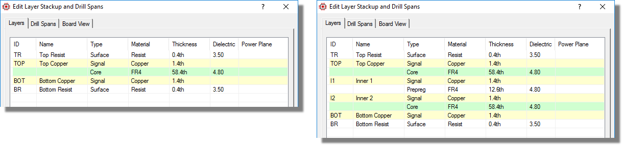
The layer stackup grid for a 2-layer board and for a 4-layer board
A Total Thickness readout beneath the grid keeps a running total of the finished board thickness as you edit the individual layer thicknesses. This is the figure to check against any mechanical constraint on the board, such as a card edge connector or an enclosure slot.
The first task when you launch this dialogue is to specify the layer stack for your PCB. For the vast majority of boards you can create your layer stack by changing a couple of parameters in the Stackup Wizard.
Stackup Wizard
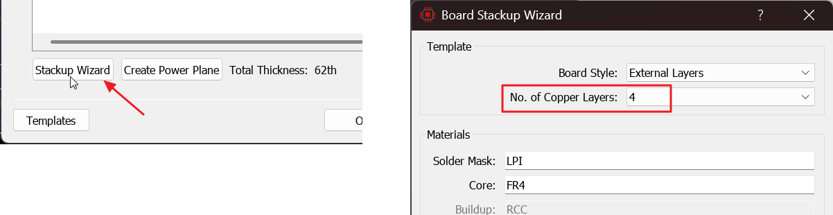
The Stackup Wizard is launched from the Stackup Wizard button on the Layers tab. It configures the number of copper layers and the board construction style, together with the materials, thicknesses and dielectric constants for each construction element.

The two most important settings are the number of copper layers and the board style. The available layer counts are constrained by the selected board style: External Layers and 1+n+1 HDI both require at least four copper layers, so lower layer counts are greyed out when either of these styles is selected. Conversely, reducing the layer count below four will reset the board style to Internal Layers. For multi-layer boards the board style selects the manufacturing construction method:
- Internal Layers - built from the inside out starting with a central core. See Internal Layer Pairs.
- External Layers - built from the outside in using multiple individually drilled cores. See External Layer Pairs.
- 1+n+1 HDI (single buildup) - a conventional core with one laser-drilled buildup layer on each side. See 1+n+1 HDI.
Together, the number of layers and the board style determine the legal set of drill spans and therefore the types of via that can be placed during manual and auto-routing. The Manufacturing and Cost Considerations section above discusses the drill constraints and engineering trade-offs for each board style in detail.
The remaining wizard fields specify materials (e.g. FR4, RCC), layer thicknesses and dielectric constants. These are used by Proteus to calculate via depth for length matching and are exported in the CADCAM readme file. For many users the default values will suffice.
Re-running the Stackup Wizard preserves your existing drill spans unless you change the number of copper layers or the board style. When the layer count or style does change, the default drill spans are recreated and any spans that match vias already placed on the board are restored automatically.
For detailed information about all the fields in the Stackup Wizard including typical thickness and dielectric ranges, see the Board Stackup Wizard dialogue help.
Editing the Grid
The grid contains the following columns.
ID
The ID is a non-editable column, providing a quick indication of the layer name.
Name
The name is an editable column where you can specify more accurate information about the use of the layer. For example, this would commonly be used with a plane layer to name the layer either VCC or GND. To edit the field, double click the mouse over the name in question and then type the replacement, hitting the enter button when done.
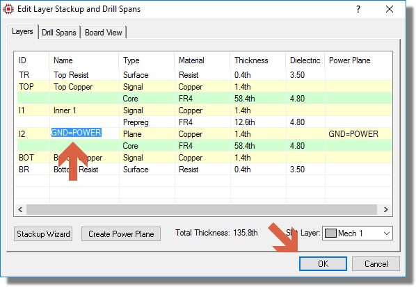
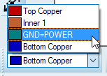
The names of the layers will then be found in the layer selector during tracking and placement operations.
Type
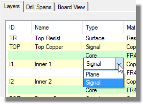
This type of layer is editable according to its function. So signal layers can be changed to be plane layers and vice versa while cores can be changed to pre-preg and vice versa. Surface layers cannot be edited.
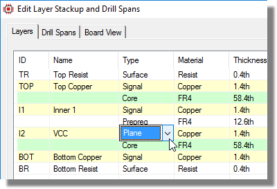
The ability to change cores and pre-preg's adds flexibility to the stackup, essentially letting you specify whatever you like. We strongly recommend that you only do this if you are comfortable with the manufacturability of the custom stackup layout and have spoken to your fab house. All standard stackups can be auto-generated from the Stackup Wizard.
A layer specified as a plane layer cannot contain tracks. If you specify a net (see below) then Proteus can both autodraw the plane and maintain distance from the board edge. The distance between the plane and the board edge is governed by the Edge clearance design rule. If you are routing on the same net as a zone on a plane layer you can simply double click the mouse to drop a via to the plane and complete the connection.
See Also:
Material
This is an editable column naming the material used for the layer, for example FR4 for a core or a pre-preg, RCC for a buildup dielectric, and the solder resist material for the surface layers. The values are set for you by the Stackup Wizard from the choices you make there, so you only need to touch this column when you are describing a material the wizard does not offer.
Like the dielectric constant, the material name is not used by Proteus itself. It is exported with the rest of the layer stack in the Gerber X2 readme.txt file, where it tells the board house exactly what you intend the board to be made from.
Thickness
This is an editable column that allows you to specify an individual thickness for a layer. To edit, first double click on the field in question, then type the new value and either hit the enter button or click the mouse elsewhere to confirm.
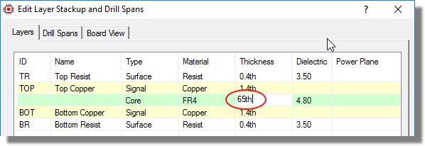
Information specified here is used by Proteus only to calculate via depth for length matching. The data is also exported along with the rest of the layer stack in the Gerber X2 readme.txt file.
Dielectric
This is an editable column that allows you to specify the dielectric constant for relevant layers. Typically, this is related to the entry in the material column. The information is not currently used in the Proteus software but is exported along with the rest of the board stackup in the Gerber X2 readme.txt file.
Power Plane
This is a read-only column that indicates when a full layer power plane has been placed on a layer. The full layer power plane might have been generated from the button just underneath the grid or from the power plane generator command on the tools menu.
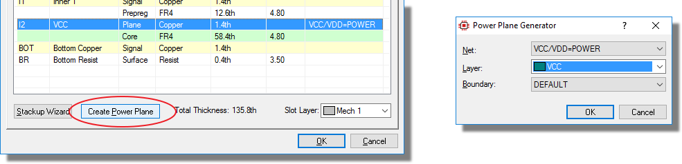
The 'Create Power Plane' is greyed out if there are no nets to attach the plane to. This is typically the case in the New Project Wizard.
It is very common to use this alongside the specification of the layer type to be a plane layer.
About Drill Spans
When a multi-layer PCB is constructed a separate pass of the drilling machine is required for each drill span. For mechanically drilled spans this is a pass of the CNC drill; for micro-via spans on HDI boards it is a pass of the laser. Having set up the layer stack there is a known legal set of drill spans which are possible. For example, in the 4-layer board discussed earlier you could have three drill spans in the case you were using two cores (external layer pairs) or two drill spans in the case you were using one core (internal layer pairs). A 1+n+1 HDI board adds micro-via spans on each side.
The tables below summarise the legal drill spans for all three construction methods at 4, 6 and 8 layers. In each case the through-hole span (Top Copper to Bottom Copper) is always present. The remaining spans depend on the board style.
4-Layer Drill Spans
| External Layer Pairs | Internal Layer Pairs | 1+n+1 HDI (n=2) |
| Top Copper to Bottom Copper | Top Copper to Bottom Copper | Top Copper to Bottom Copper |
| Top Copper to Inner 1 (blind) | Inner 1 to Inner 2 (buried) | Top Copper to Inner 1 (micro-via) |
| Inner 2 to Bottom Copper (blind) | Inner 1 to Inner 2 (buried) | |
| Inner 2 to Bottom Copper (micro-via) |
6-Layer Drill Spans
| External Layer Pairs | Internal Layer Pairs | 1+n+1 HDI (n=4) |
| Top Copper to Bottom Copper | Top Copper to Bottom Copper | Top Copper to Bottom Copper |
| Top Copper to Inner 1 (blind) | Inner 1 to Inner 2 (buried) | Top Copper to Inner 1 (micro-via) |
| Inner 2 to Inner 3 (buried) | Inner 3 to Inner 4 (buried) | Inner 1 to Inner 2 (buried) |
| Inner 4 to Bottom Copper (blind) | Inner 3 to Inner 4 (buried) | |
| Inner 4 to Bottom Copper (micro-via) |
8-Layer Drill Spans
| External Layer Pairs | Internal Layer Pairs | 1+n+1 HDI (n=6) |
| Top Copper to Bottom Copper | Top Copper to Bottom Copper | Top Copper to Bottom Copper |
| Top Copper to Inner 1 (blind) | Inner 1 to Inner 2 (buried) | Top Copper to Inner 1 (micro-via) |
| Inner 2 to Inner 3 (buried) | Inner 3 to Inner 4 (buried) | Inner 1 to Inner 2 (buried) |
| Inner 4 to Inner 5 (buried) | Inner 5 to Inner 6 (buried) | Inner 3 to Inner 4 (buried) |
| Inner 6 to Bottom Copper (blind) | Inner 5 to Inner 6 (buried) | |
| Inner 6 to Bottom Copper (micro-via) |
The method and the sequence in which the multi-layer board is assembled directly affect the available drill spans. If the tables above are not clear, refer to the construction diagrams in the About Layer Stacks section and the worked examples in Manufacturing and Cost Considerations.
1+n+1 HDI Inner Core Construction
In the tables above, the 'n' in 1+n+1 refers to the number of inner copper layers between the two buildup layers (n=2 for a 4-layer board, n=4 for 6-layer, n=6 for 8-layer). The inner core section is constructed using alternating cores and pre-preg in the same dielectric pattern as external layer pairs: each core is an independently drillable pair of copper layers. This is why the mechanical buried via spans within the inner core always connect adjacent pairs of inner layers across a single core (e.g. Inner 1 to Inner 2, Inner 3 to Inner 4).
The micro-via spans on each side use laser drilling at typical diameters of 0.1 mm (4 mil) and can only span a single buildup layer. The inner core buried via spans use conventional mechanical drilling at standard sizes of 0.2 mm (8 mil) and above.
The Stackup Wizard automatically creates the micro-via spans and the through-hole span for HDI boards. To add the inner core buried via spans listed in the tables above, use the 'Create from Cores' button in the Drill Spans tab. See Defining Drill Spans for further details.
Key Points
- Possible drill spans are determined by the layer stack and board style.
- Mechanical drill spans use CNC drilling; micro-via spans use laser drilling.
- When placing a route with a via, the via will acquire the shortest drill span that allows the track to go from source layer to destination layer. The available drill spans for vias are defined here.
Defining Drill Spans
Drill spans are defined in the Drill Spans tab of the layer stackup dialogue. There are two approaches: automatic generation using the buttons beneath the grid, or manual addition of individual spans.
Automatic Generation
The Stackup Wizard always creates a through-hole drill span (Top Copper to Bottom Copper). For 1+n+1 HDI boards it also creates the micro-via spans on each side (e.g. Top Copper to Inner 1 and Inner n to Bottom Copper). All other spans must be added separately, either automatically or manually.
The 'Create from Cores' button will auto-generate a full set of mechanically drilled spans based on the cores in the layer stackup. This is the recommended way to add blind and buried via spans. For a conventional board (internal or external layer pairs) this is usually sufficient. For a 1+n+1 HDI board it adds the buried inner core spans to complement the micro-via spans already created by the wizard.
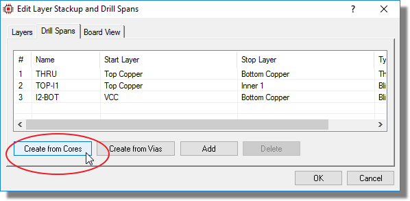
The 'Create from Vias' button caters for legacy designs and will create drill spans to match the vias already placed on the board.
After generating spans you should review the list and delete any that are not needed. Each drill span represents a pass of the drilling machine and adds to fabrication cost, so it is good practice to include only those spans that your design actually requires.
Manual Addition
Individual drill spans can be added using the Add button. The Add Drill Span dialogue allows you to specify the start (from) and end (to) copper layers for the span.
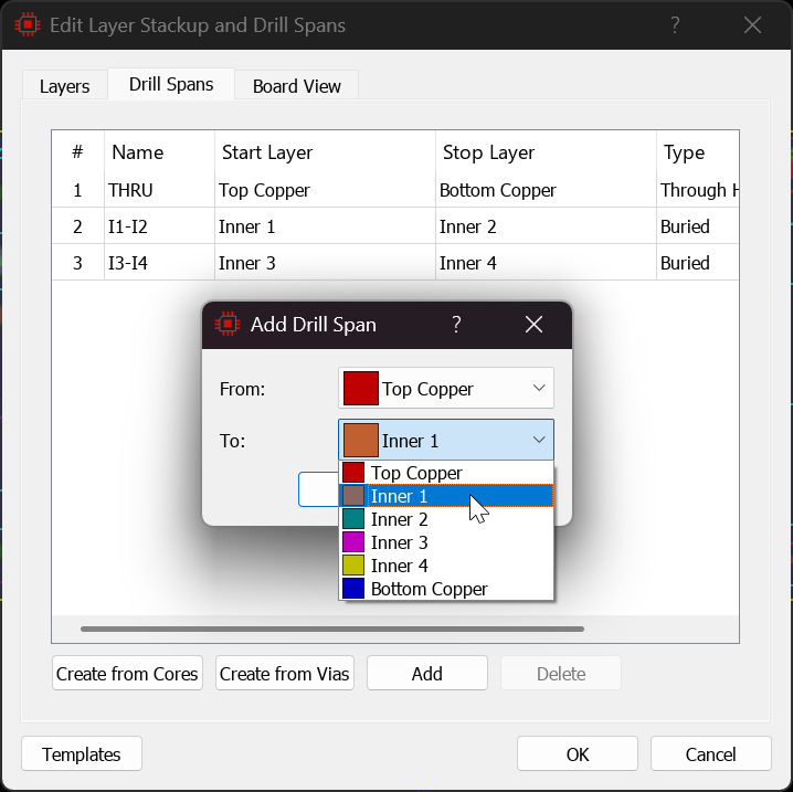
Adding a drill span by naming its start and end copper layers
Automatic Micro-Via Detection
Proteus automatically determines whether a manually added span is a micro-via or a mechanical drill span based on the layer topology. If the selected start and end layers are adjacent copper layers separated by a buildup dielectric (e.g. Top Copper to Inner 1, or Inner n to Bottom Copper on a 1+n+1 HDI board), the span is created as a laser-drilled micro-via. All other layer combinations produce a mechanical CNC drill span. A given layer pair can only have one drill span; you cannot have both a CNC span and a laser span between the same two layers.
For most 1+n+1 HDI designs, the micro-via spans are created automatically by the Stackup Wizard and the inner core spans are added using 'Create from Cores'. Manual addition is useful when you have deleted a span and need to re-add it, or when building an unusual stackup.
Validation
Proteus performs sanity checks on the drill span set, warning you if a manually added span conflicts with existing spans or is not manufacturable with standard techniques. The most common cause of warnings is overlapping partial drill spans (e.g. Top Copper to Inner 3 combined with Bottom Copper to Inner 2) which would require drilling from both sides into the middle of the board.
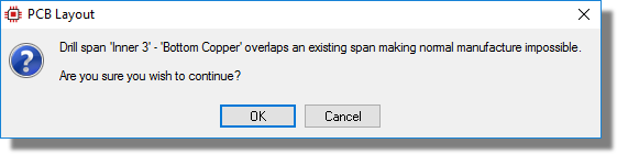
You can override these warnings if your board manufacturer is comfortable with the construction, but we recommend discussing any non-standard drill span arrangement with your fabricator before committing to it.
You can remove any drill spans that you do not need apart from the through-hole span which is always required. If the span you are deleting is in use by vias already placed on the board then a separate confirmation is raised first, since those vias will have to be re-assigned to another span. Bear in mind that when you place a via during routing, Proteus automatically selects the shortest compatible drill span that covers the source and destination layers. Every defined mechanical span is potentially used, so include only those you actually want.
Smart Vias & Layer Pairs
The configuration of the layer stack and the drill spans is important because it makes life much easier when you are routing the board. In particular, Proteus knows the valid ways in which you are allowed to move between layers and so can make intelligent decisions when a via is placed. This includes automatically selecting the correct drill span type based on both the stackup and the active via pad style. All that is left is to tell Proteus which signal layer you want to arrive on when you via from a specific layer and this is done via the layer pairs dialogue on the Technology menu.
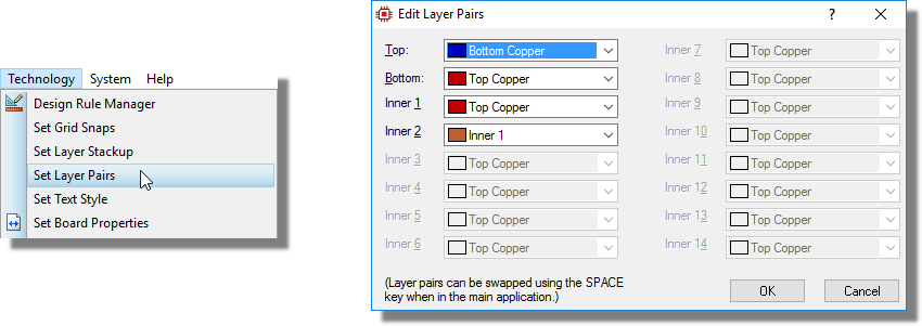
The layer pairs dialogue on the Technology menu
The idea behind layer pairs is to allow you to create associations between layers. This is useful for example when laying tracks: double clicking the mouse will automatically create a via from the current layer to its associated layer and continue tracking on that layer. To change a layer pair select a layer from the drop down list that you wish to associate with the layer specified by the text on the left.
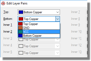
It is not uncommon for much of this dialogue to be greyed out; you cannot create associations between layers not in the stackup. Also, only signal layers are shown here because you cannot place tracks on plane layers.
Manual Routing
When you are placing a route you can switch layers by double clicking the mouse. This will drop a via so that you can keep routing without interruption on the destination layer. With smart vias enabled, Proteus automatically selects the most appropriate drill span for the layer transition. The via pad style and drill span chosen at this point are defaults, and you can always edit a via after placement to change its pad style or drill span. The default selection process is as follows:
- The layer pairs define which layer you want to arrive on when you double click from a given layer.
- The default via pad style is taken from a DRC Room if one is present at the via location, or from the net class otherwise. Micro-via pad styles are not available in the net class dialogue, so the only way to place micro-vias during routing is through a DRC Room.
- The smart via algorithm finds the shortest drill span that covers the source and destination layers and is compatible with the default via pad style. If the pad style is a micro-via style, micro-via drill spans are considered. If it is a standard mechanical style, only mechanical drill spans (blind, buried, through-hole) are considered.
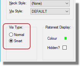
It is important to understand that every mechanical drill span you define is a candidate for automatic selection. If your stackup includes blind or buried spans then these will be used in preference to through-hole wherever they provide a shorter path between the source and destination layers. Micro-via spans are only selected when the via pad style is a micro-via style. Since micro-via pad styles are not available in the net class dialogue, this means micro-via placement during routing is controlled exclusively by DRC Rooms. You can control smart via selection on a per-net-class basis: setting the via type to Normal in the net class tab forces all vias to through-hole for that net class, whilst Smart enables automatic span selection.
On HDI boards, a DRC Room with a micro-via pad style is the only mechanism that enables micro-via placement during routing. Without a DRC Room, the net class via style is always a standard mechanical via (since micro-via styles cannot be selected in the net class dialogue) and the smart via algorithm will select the shortest mechanical drill span, bypassing the micro-via spans entirely. This means you can safely route standard nets across the board without worrying about accidentally placing micro-vias.
Example: External Layers 6-Layer Board
Setup:
- Board style: External Layer Pairs, 6 copper layers.
- Drill spans: Through-hole, Top Copper to Inner 1 (blind), Inner 2 to Inner 3 (buried), Inner 4 to Bottom Copper (blind).
- Layer pairs: Top Copper ↔ Inner 1, Inner 1 ↔ Inner 2.
- Net class: smart vias enabled, via style C30 (standard mechanical via).
When routing on Top Copper, a double click transitions to Inner 1. The smart via algorithm finds that the Top Copper to Inner 1 blind span is shorter than through-hole and selects it. A C30 blind via is placed. If you then double click again to transition from Inner 1 to Inner 2, there is no blind or buried span covering exactly Inner 1 to Inner 2, so the through-hole span is used and a C30 through-hole via is placed.
Example: 1+n+1 HDI 6-Layer Board (Standard Via Style)
Setup:
- Board style: 1+n+1 HDI, 6 copper layers.
- Drill spans: Through-hole, Top Copper to Inner 1 (micro-via), Inner 1 to Inner 2 (buried), Inner 3 to Inner 4 (buried), Inner 4 to Bottom Copper (micro-via).
- Layer pairs: Top Copper ↔ Inner 1.
- Net class: smart vias enabled, via style C30 (standard mechanical via). No DRC Room.
When routing on Top Copper and double clicking to transition to Inner 1, the smart via algorithm detects that C30 is a standard mechanical via style and excludes micro-via spans from consideration. The shortest mechanical span covering Top Copper to Inner 1 is the through-hole span, so a C30 through-hole via is placed. If you need this via to be a micro-via instead, you can edit it after placement to change the pad style and drill span.
Example: 1+n+1 HDI 6-Layer Board (DRC Room With Micro-Via Style)
Setup:
- Board style: 1+n+1 HDI, 6 copper layers.
- Drill spans: Through-hole, Top Copper to Inner 1 (micro-via), Inner 1 to Inner 2 (buried), Inner 3 to Inner 4 (buried), Inner 4 to Bottom Copper (micro-via).
- Layer pairs: Top Copper ↔ Inner 1.
- Net class: smart vias enabled, via style C30 (standard mechanical via). DRC Room with micro-via pad style placed under BGA.
When routing on Top Copper and double clicking inside the DRC Room to transition to Inner 1, the DRC Room overrides the net class via style with the micro-via pad style. The smart via algorithm detects that this is a micro-via style and includes micro-via spans in its search. The Top Copper to Inner 1 micro-via span is shorter than through-hole and is selected. A micro-via is placed correctly. When double clicking outside the DRC Room on the same layer transition, C30 applies as in the previous example and a through-hole via is placed.
On HDI boards, the DRC Room is the mechanism that controls where micro-vias are placed. The net class provides the default mechanical via style for general routing, and DRC Rooms with micro-via pad styles enable micro-via placement in specific areas such as under BGA footprints. This two-tier approach means you can route freely across the board: micro-vias are placed inside DRC Rooms and standard mechanical vias are placed everywhere else.
Example: Micro-Vias Needed Along an Entire Net
Occasionally you may need micro-vias at every layer transition along a particular net rather than just within a specific area. Micro-via pad styles cannot be set in the net class dialogue, so the route to take is still the DRC Room, using the Apply Style button on the room dialogue to retro-fit the style to vias that have already been placed:
- Route the net as normal with smart vias enabled. Mechanical vias will be placed at each layer transition.
- Draw a DRC Room covering the run of the net, set its via style override to your micro-via pad style and tick the Use Microvia checkbox.
- Click Apply Style. The room applies its via style to every via already inside it, so the whole run is converted in a single operation.
For the occasional via that falls outside any room, right click on it and use the edit via command to change both its pad style and its drill span by hand.
Either route works provided the routed layer transitions correspond to valid micro-via drill spans in the stackup, that is adjacent copper layers across a buildup dielectric. Proteus will not allow you to assign a micro-via drill span to a via that bridges layers which cannot be laser drilled.
You can also place a via by pressing the SPACE bar during routing. The process is a little more involved and works as follows:
- User is placing a track and hits the SPACE bar to float a via on the end of the track.
- User presses PGUP and PGDN to cycle through the valid layer destinations for the via.
- User clicks the left mouse to drop the via and continue routing on the destination layer. With smart vias enabled the best drill span for the chosen destination is selected automatically at the end.
The same smart via span selection applies to floating vias. While slightly more time consuming there are times where the floating via method is the better choice. If space is tight on the PCB the floating via is DRC aware and you will not be allowed to place a via in an illegal spot. Also, since you can choose the destination routing layer interactively it is well suited for escaping BGAs and other tricky routing problems where it is not clear what layer you will be using until you are in the process of routing.
Connecting to Plane Layers
Since plane layers cannot contain tracking the procedure for connecting to a plane layer is even simpler. If you are placing a track and want to connect to a plane layer the only thing you need to do is double click the mouse anywhere over (or under) the plane. In this case, Proteus is doing the following:
- Checking the net of the track that you are routing (e.g. VCC).
- Looking down (and up) from the layer you are on to find a plane layer on the same net. Plane layers are defined in the layer stackup.
- Placing a via to the plane layer and terminating the route.
See Also:
Auto-routing
There are a couple of differences between auto-routing and manual routing. First, you specify the layer pairs in the net class tab of the design rule manager. This has the added benefit of enabling different layer pairings for different net classes.
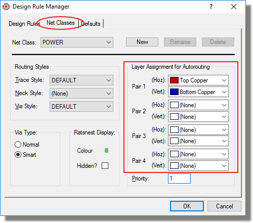
You also have a choice on a net class basis to decide between normal vias and smart vias. A normal via will always be through-hole whereas a smart via will use the shortest mechanical drill span available to get the track from the source layer to the destination layer.
The auto-router places standard mechanical vias only. It will not place micro-vias, and it does not honour the micro-via style on a DRC Room while it is routing. The remedy is to autoroute the board first and then use the Apply Style button on the DRC Room to apply the micro-via style to the vias the autorouter has left inside it. On 1+n+1 HDI boards, that is the practical way to get micro-vias into a BGA escape area after autorouting.
Via Mode
You can place a via manually by selecting via mode from the mode selector. When you do this the layer selector will switch to show the valid drill spans for vias as defined by the layer stackup. Select the one you want and then left click to place the via.

Editing Vias
The via pad style and drill span assigned during route placement are defaults, not permanent constraints. You can right click on any placed via and use the edit via command to change its pad style, drill span or both. This is useful when you need to override the automatic selection for a specific via, for example changing a through-hole via to a micro-via on a layer transition that supports laser drilling.
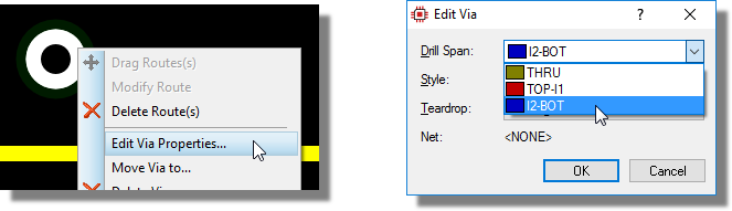
Editing the pad style and drill span of a placed via
The dialogue carries its own Microvia checkbox. Ticking it filters both the via style list and the drill span list down to the micro-via entries, which is the quickest way to find the right combination and also stops you from pairing a micro-via style with a mechanical span. Two constraints are applied automatically once the via is a micro-via: the hole size is held between 3 thou and 8 thou, and via filling is forced on and greyed out, because micro-vias are copper filled as part of the HDI fabrication process.
If you tick the Microvia checkbox on a via whose current span crosses more than one dielectric, Proteus warns you that micro-vias can only span adjacent layers and that you will need to choose a different drill span. Check connectivity afterwards, since shortening the span may break a connection the original via was making.
Micro-Via Pad Styles and DRC Rooms
Micro-vias have different physical dimensions from standard mechanical vias and therefore require their own pad styles. A micro-via pad style is a via design that has the micro-via flag set, indicating that it uses laser drilling. Micro-via pad styles are excluded from the net class via style selector because micro-vias are inherently regional on the board: they apply to specific layer transitions at specific locations rather than uniformly to an entire net class. This separation also prevents mismatches between via styles and drill span types.
The mechanism for controlling which via pad style is used at a given location on the board is the DRC Room. A DRC Room is a rectangular or polygonal region on the board that overrides design rules within its boundary. For HDI designs, the typical workflow is:
- Define a micro-via pad style with the appropriate hole size and pad geometry (typically 0.1 mm hole, 0.25 mm pad).
- Tick the Use Microvia checkbox on the room dialogue. Until you do, the Via Style selector will not offer micro-via styles at all, so this step comes before you can pick one.
- Draw a DRC Room around the area where micro-vias are needed (e.g. under and around a fine-pitch BGA).
- Assign the micro-via pad style to the DRC Room as its via style override.
The Use Microvia checkbox also validates the layer span, so it will not let you pair a micro-via style with a transition that cannot be laser drilled. The checkbox is disabled, with a tooltip explaining why, when the board stackup is not HDI capable or when no micro-via styles have been defined yet.
The room dialogue also carries an Apply Style button, which applies the selected via style to every via already inside the room. This is how you retro-fit micro-vias to a region that has already been routed, whether by hand or by the autorouter.
When a via is placed inside the DRC Room, the room's micro-via pad style overrides the net class default. Because the pad style is now a micro-via style, the smart via algorithm includes micro-via drill spans in its search and will select them where they are the shortest available span. If the layer transition does not correspond to a valid micro-via drill span, for example a through-hole transition across the full board, the override is not applied at all: the via falls back to the net class via style and its mechanical drill span, and a one-shot warning is reported on the status bar.
DRC Rooms are particularly useful for BGA escape routing on HDI boards. By placing a room under the BGA footprint and assigning a micro-via pad style, all vias placed within the BGA area on the buildup layer spans will automatically use the correct micro-via geometry.
Key Points
- Correct setup of the layer stack and the layer pairs will save a huge amount of time during the routing phase of the project.
- If you add a mechanical drill span, Proteus will use it automatically during manual routing.
- The smart via algorithm considers the via pad style when selecting drill spans. Micro-via spans are only selected when the via pad style is a micro-via style; a standard via style will always use the shortest mechanical span.
- On HDI boards, DRC Rooms with micro-via pad styles control where micro-vias are placed. Outside of DRC Rooms, standard mechanical vias are used regardless of whether micro-via drill spans exist in the stackup.
- The auto-router places standard mechanical vias only. Micro-vias must be placed manually or through DRC Room overrides.
- The via pad style and drill span chosen during placement are defaults. You can edit any via after placement to change its pad style or drill span as needed.
Custom Layer Stacks
The Stackup Wizard provides a simple and fast way to configure boards for production using standard techniques. Of course, the designer knows best and there are good reasons to create custom stackups. Proteus will allow you to do this as follows:
1) Use the Stackup Wizard to specify the number of layers.
2) Edit the type fields for the cores and pre-pregs to form the desired stackup.
3) Edit the thickness fields as appropriate.
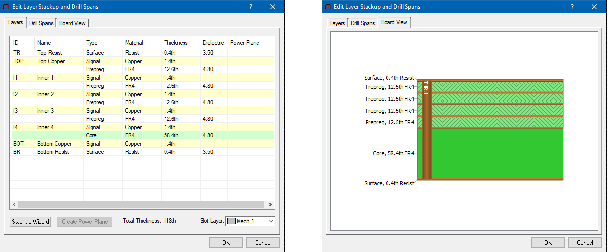
For example, the 6-layer board below has a stackup normally called 'build-up' comprised of one core and then successive applications of pre-preg plus copper foil. This was created by specifying a 6-layer board (external pairs) and then changing the top two cores to be pre-preg.
We strongly recommend that you discuss any custom stackup with your board manufacturer both for feasibility and for cost.